German President, Pyeongtaek Samsung Electronics Visit… Semiconductor Cooperation Discussion
Frankfurter Stein Meier, the German president, visited Samsung Electronics' Pyeongtaek Campus in Pyeongtaek, Gyeonggi-do, to discuss ways to cooperate with Samsung Electronics.
The president of Stein Meier visited Samsung Electronics Pyeongtaek Campus Semiconductor 1 (P1) this morning.
This is the first time the German president has officially visited Samsung Electronics. President Stein MER Ear signed a memory semiconductor silicon disc at Samsung Electronics' Pyeongtaek Campus.
 In addition to the German presidents, about 60 people from Germany, including the German Federal House of Representatives, the economic and cultural personnel, journalists, and attendants, visited Samsung Electronics' Pyeongtaek Campus. In Samsung Electronics, CEO Gyeong-hyun, CEO (President) and Choir Si-young Foundry Business Division (President) welcomed them.
Samsung Electronics' Pyeongtaek Campus is a large complex with a total area of 2.89 million square meters (about 870,000 pylons). It is the sum of 400 soccer fields. Samsung Electronics has both memory semiconductor production lines and system semiconductor consignment production (foundry) facilities on Pyeongtaek Campus.
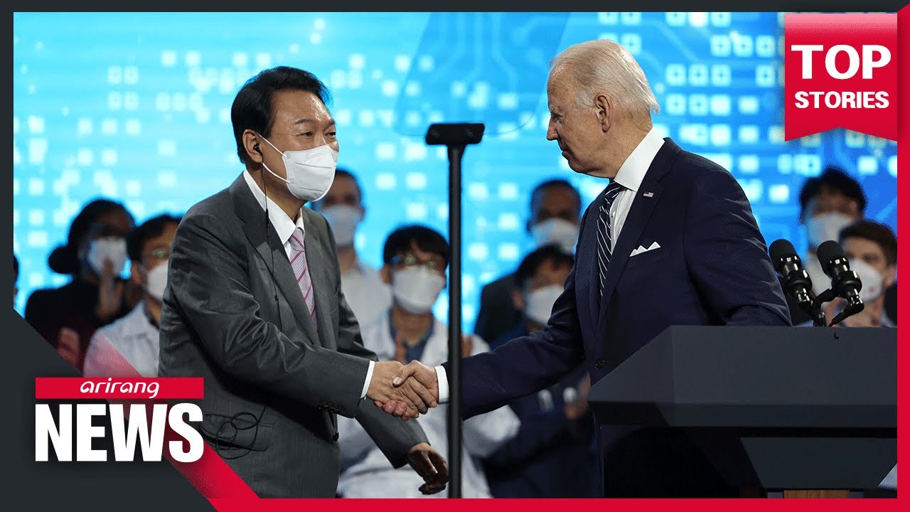
It is also a place where President Soon Seok-yeol and US President Joe Biden signed a three-nanometer (nm and 1 nm 1 billion) foundry process prototype. President Biden visited Samsung Electronics' Pyeongtaek Campus on May 20 as a first schedule for visit. Lee Jae-young, vice chairman of Samsung Electronics, introduced the world's first high-tech semiconductor.


Comments
Post a Comment